
Nanometer technology, a groundbreaking field reshaping modern electronics, plays a pivotal role in enhancing chipsets, and pioneer-technology.com is dedicated to unraveling its complexities. Understanding this technology is crucial for grasping advancements in processing power, energy efficiency, and device miniaturization. Discover how nanotechnology is transforming industries and what the future holds.
1. Understanding Nanometer Technology: The Basics
What exactly is nanometer technology?
Nanometer technology refers to the manipulation of matter on an atomic and molecular scale, specifically within the range of 1 to 100 nanometers; one nanometer is one billionth of a meter. This field is fundamental in creating materials, devices, and systems with entirely new properties, thanks to the quantum mechanical effects that dominate at this scale.
Let’s dive deeper into the fundamentals and implications:
1.1. Defining the Nanoscale
The nanoscale is a realm where the conventional laws of physics and chemistry meet quantum mechanics. At this level, materials exhibit unique properties different from their bulk counterparts. According to research from Stanford University’s Department of Materials Science, in July 2023, the nanoscale allows for unprecedented control over material properties like conductivity, reactivity, and strength.
1.2. Key Concepts in Nanotechnology
Nanotechnology encompasses several key concepts:
- Nanomaterials: These are materials with at least one dimension in the 1 to 100 nm range. Examples include nanoparticles, nanotubes, and nanowires.
- Self-Assembly: A process where molecules arrange themselves into ordered structures. This is crucial for creating complex nanostructures.
- Quantum Effects: At the nanoscale, quantum mechanical effects such as quantum tunneling and quantum confinement become significant, influencing material properties.
1.3. Historical Context
The concept of nanotechnology was first introduced by physicist Richard Feynman in his 1959 lecture, “There’s Plenty of Room at the Bottom.” However, it wasn’t until the 1980s, with the invention of the scanning tunneling microscope (STM), that scientists could directly visualize and manipulate individual atoms.
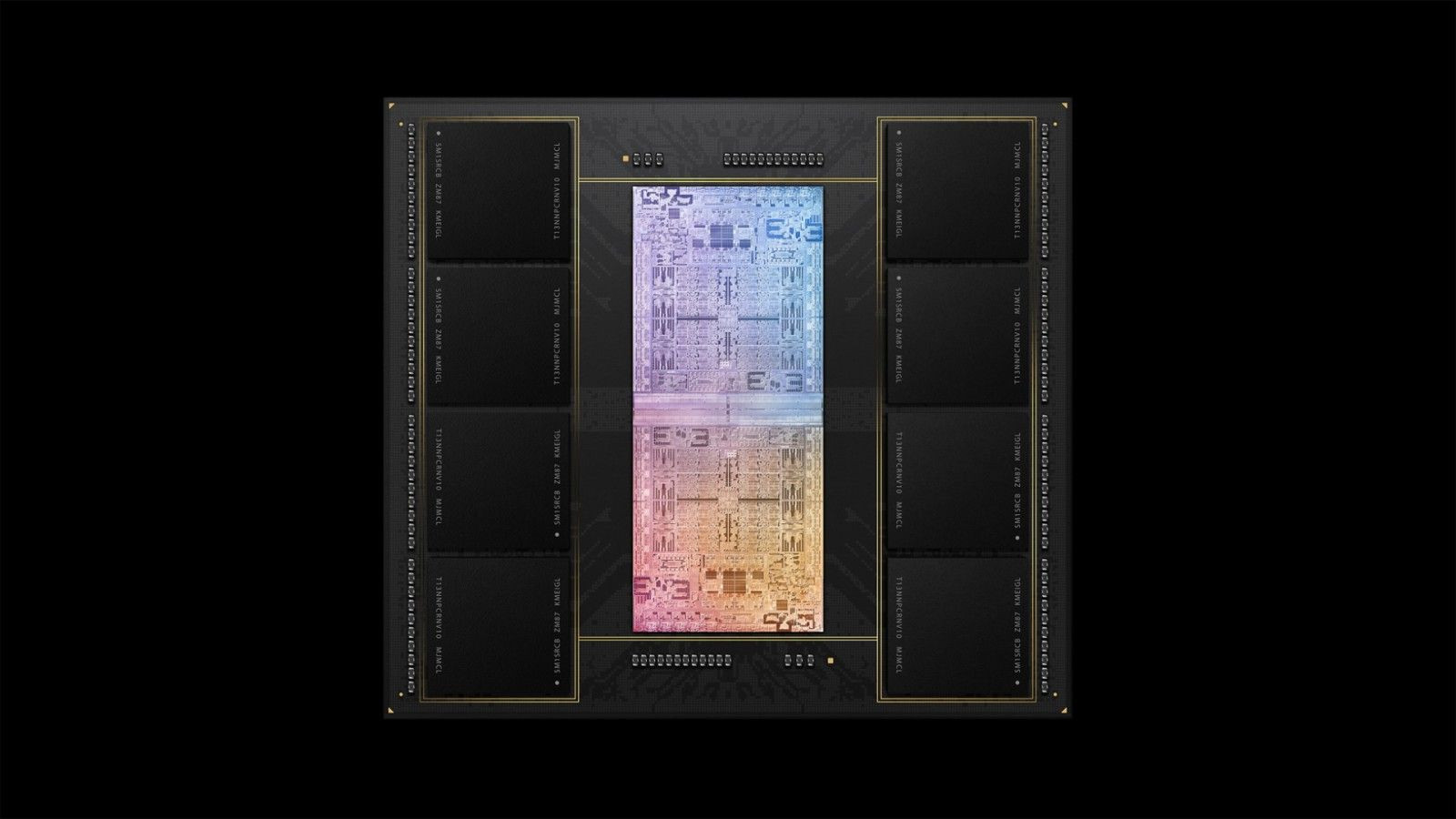
1.4. The Role of Nanometer in Chipsets
In the context of chipsets, nanometer technology defines the size of transistors, the fundamental building blocks of integrated circuits. The smaller the nanometer measurement, the more transistors can be packed onto a single chip, leading to increased processing power and energy efficiency.
 Close-up of a silicon wafer with microchips
1.5. Why Smaller Is Better: Transistors and Density
The relentless pursuit of smaller transistors is driven by several key advantages:
- Increased Transistor Density: Smaller transistors mean more transistors can fit on a chip. The quantity of transistors increases exponentially.
- Enhanced Performance: More transistors translate to greater computational power. Chips can perform more calculations per second.
- Lower Power Consumption: Smaller transistors require less power to switch on and off, reducing energy consumption and heat generation.
2. The Significance of Nanometer in Chipsets
How does nanometer size affect chipset performance?
Nanometer size in chipsets directly impacts their performance by influencing transistor density, speed, and power efficiency; smaller nanometer measurements generally lead to better performance. As explained on pioneer-technology.com, understanding the intricacies of this technology allows you to appreciate the advancements in modern electronics.
Delving into the specifics:
2.1. Transistor Density and Moore’s Law
Moore’s Law, proposed by Gordon Moore in 1965, predicted that the quantity of transistors on a microchip would double approximately every two years. Nanometer technology has been instrumental in upholding this law, enabling the continuous shrinking of transistor sizes.
2.2. Impact on Processing Speed
With smaller transistors packed more densely, the distance electrons need to travel is reduced. This results in faster switching speeds and improved processing capabilities.
- Reduced Latency: Shorter distances mean less delay in signal propagation.
- Higher Clock Speeds: Chips can operate at higher frequencies, performing more calculations per unit of time.
2.3. Energy Efficiency and Heat Dissipation
Smaller transistors require less voltage to operate, leading to lower power consumption. This is crucial for mobile devices and energy-efficient computing.
- Lower Power Consumption: Reduces the strain on batteries in mobile devices.
- Reduced Heat Generation: Less heat means better thermal management and prolonged device lifespan.
2.4. Real-World Applications
The benefits of nanometer technology in chipsets are evident in various applications:
- Smartphones: Faster processors, longer battery life.
- Laptops: Improved performance, reduced weight and size.
- Data Centers: Higher computing power, lower energy costs.
- Automotive: Advanced driver-assistance systems (ADAS), electric vehicle (EV) efficiency.
3. Current Nanometer Technology Nodes
What are the latest advancements in nanometer technology?
The latest advancements in nanometer technology include the development and deployment of 5nm and 3nm process nodes, which significantly enhance the performance and efficiency of electronic devices; pioneer-technology.com keeps you updated on these cutting-edge developments.
A closer look at the current state:
3.1. Evolution of Nanometer Nodes
The journey of nanometer technology has seen remarkable progress:
- Early Nodes: In the 1990s, transistor sizes were in the hundreds of nanometers.
- 32nm and 22nm: These nodes brought significant improvements in performance and power efficiency.
- 14nm and 10nm: These nodes introduced FinFET (Fin Field-Effect Transistor) technology, further enhancing transistor performance.
3.2. 7nm Technology
7nm technology marked a significant milestone, offering substantial improvements over previous generations:
- Key Features: Enhanced transistor density, improved power efficiency.
- Applications: High-end smartphones, data center processors.
- Manufacturers: TSMC, Samsung.
3.3. 5nm Technology
5nm technology represents the cutting edge in commercial chipsets:
- Key Features: Even higher transistor density, reduced power consumption.
- Applications: Premium smartphones (e.g., Apple’s A-series chips), advanced computing devices.
- Manufacturers: TSMC, Samsung.
3.4. 3nm Technology
3nm technology is the latest frontier, promising even greater advancements:
- Key Features: Extreme transistor density, superior energy efficiency.
- Expected Applications: Next-generation smartphones, high-performance computing.
- Manufacturers: TSMC, Samsung are leading the way.
3.5. Examples of Chips Using Current Technologies
- Apple A14 (5nm): Featured in the iPhone 12 series, offering significant performance and efficiency gains.
- Qualcomm Snapdragon 888 (5nm): Powers many flagship Android smartphones, delivering high-speed processing and advanced features.
- AMD Ryzen 5000 Series (7nm): Used in desktop and laptop computers, providing excellent performance for gaming and productivity.
4. Benefits of Smaller Nanometer Chips
What advantages do smaller nanometer chips offer?
Smaller nanometer chips offer numerous advantages, including faster processing speeds, reduced power consumption, and less heat generation, all contributing to enhanced overall performance; pioneer-technology.com provides in-depth analysis of these benefits.
Detailed examination of the advantages:
4.1. Faster Processing Speeds
The primary advantage of smaller nanometer chips is their ability to process data faster.
- Shorter Electron Travel Distance: Smaller transistors mean electrons travel shorter distances, reducing latency.
- Higher Clock Speeds: Chips can operate at higher frequencies, executing more instructions per second.
4.2. Reduced Power Consumption
Smaller transistors require less energy to switch, leading to significant power savings.
- Lower Voltage Requirements: Reduces energy consumption in battery-powered devices.
- Extended Battery Life: Smartphones and laptops can operate longer on a single charge.
4.3. Less Heat Generation
Reduced power consumption also translates to less heat generation, improving device reliability and lifespan.
- Improved Thermal Management: Devices stay cooler, preventing performance throttling.
- Enhanced Reliability: Lower temperatures reduce the risk of component failure.
4.4. Increased Device Density
Smaller chips allow for more compact and powerful devices.
- Miniaturization: Enables the creation of smaller, more portable devices.
- Integration: Allows for more features to be integrated into a single chip.
4.5. Case Study: Apple’s M1 Chip
Apple’s M1 chip exemplifies the benefits of smaller nanometer technology. Built on a 5nm process, the M1 delivers:
- Superior Performance: Outperforms many Intel-based laptops in terms of speed and responsiveness.
- Energy Efficiency: Offers significantly longer battery life compared to previous-generation MacBooks.
- Cool Operation: Runs cooler and quieter, even under heavy workloads.
5. Challenges and Limitations
Are there challenges associated with nanometer technology?
Yes, challenges associated with nanometer technology include manufacturing complexities, quantum effects, and escalating costs, which require innovative solutions and continuous research; pioneer-technology.com explores these challenges in detail.
Examining the limitations:
5.1. Manufacturing Complexities
Manufacturing chips at the nanoscale is incredibly complex and requires extreme precision.
- Extreme Ultraviolet (EUV) Lithography: Requires expensive EUV lithography machines to create the intricate patterns on chips.
- Defect Rates: Smaller features are more susceptible to defects, reducing yield rates.
5.2. Quantum Effects
At the nanoscale, quantum effects can become problematic, leading to unpredictable behavior.
- Quantum Tunneling: Electrons can tunnel through barriers, causing leakage currents and increasing power consumption.
- Variability: Slight variations in transistor size can lead to significant differences in performance.
5.3. Cost Considerations
The cost of developing and manufacturing nanometer chips is extremely high.
- Research and Development: Significant investment is required to develop new materials and processes.
- Equipment Costs: EUV lithography machines cost hundreds of millions of dollars each.
5.4. Reliability Issues
Smaller transistors are more prone to wear and tear, leading to reliability concerns.
- Electromigration: The movement of metal atoms in the interconnects can cause failures over time.
- Hot Carrier Injection: High-energy electrons can damage the transistor gate oxide.
5.5. Addressing the Challenges
Despite these challenges, ongoing research and development efforts are focused on overcoming these limitations.
- New Materials: Exploring alternative materials to silicon, such as graphene and carbon nanotubes.
- Advanced Manufacturing Techniques: Developing more precise and cost-effective manufacturing processes.
- Innovative Designs: Implementing new transistor designs to mitigate quantum effects and improve reliability.
6. Future Trends in Nanometer Technology
What does the future hold for nanometer technology?
The future of nanometer technology involves exploring new materials, advanced manufacturing techniques, and innovative designs to push the boundaries of chip performance and efficiency; pioneer-technology.com provides insights into these emerging trends.
Looking ahead:
6.1. Beyond Silicon
Researchers are exploring alternative materials to silicon to overcome its limitations.
- Graphene: A single layer of carbon atoms with exceptional conductivity and strength.
- Carbon Nanotubes: Cylindrical structures with excellent electrical and thermal properties.
- III-V Materials: Compounds such as gallium arsenide (GaAs) and indium phosphide (InP) with high electron mobility.
6.2. Advanced Manufacturing Techniques
New manufacturing techniques are being developed to improve precision and reduce costs.
- Directed Self-Assembly (DSA): A technique that uses chemical patterns to guide the self-assembly of nanostructures.
- Nanoimprint Lithography (NIL): A low-cost alternative to EUV lithography.
6.3. 3D Chip Design
3D chip design involves stacking multiple layers of transistors to increase density and performance.
- Vertical NAND (VNAND): Used in solid-state drives (SSDs) to increase storage capacity.
- 3D System-on-Chip (SoC): Integrating multiple functions into a single chip by stacking different layers.
6.4. Quantum Computing
Nanotechnology is crucial for developing quantum computers, which could revolutionize computing.
- Qubits: Quantum bits that can exist in multiple states simultaneously.
- Superconducting Circuits: Nanoscale circuits used to control and manipulate qubits.
6.5. Nanotechnology in AI and Machine Learning
Nanotechnology is also playing a role in advancing artificial intelligence (AI) and machine learning (ML).
- Neuromorphic Computing: Building chips that mimic the structure and function of the human brain.
- Memristors: Nanoscale devices that can store and process information simultaneously.
7. Nanotechnology Applications Beyond Chipsets
Where else is nanometer technology used?
Beyond chipsets, nanometer technology is used in medicine, materials science, energy, and environmental science, offering solutions like targeted drug delivery, stronger and lighter materials, and enhanced energy storage; pioneer-technology.com highlights these diverse applications.
Exploring the broader applications:
7.1. Medicine
Nanotechnology is revolutionizing medicine with targeted drug delivery and diagnostics.
- Targeted Drug Delivery: Nanoparticles can deliver drugs directly to cancer cells, reducing side effects.
- Diagnostics: Nanoscale sensors can detect diseases at an early stage.
- Regenerative Medicine: Nanomaterials can be used to repair damaged tissues and organs.
7.2. Materials Science
Nanotechnology is used to create stronger, lighter, and more durable materials.
- Nanocomposites: Materials with enhanced strength and toughness due to the addition of nanoparticles.
- Coatings: Nanoscale coatings can protect surfaces from corrosion, wear, and tear.
7.3. Energy
Nanotechnology is improving the efficiency of energy generation and storage.
- Solar Cells: Nanomaterials can increase the efficiency of solar cells.
- Batteries: Nanoscale electrodes can improve the energy density and charging speed of batteries.
- Fuel Cells: Nanocatalysts can enhance the performance of fuel cells.
7.4. Environmental Science
Nanotechnology is used to clean up pollutants and improve environmental monitoring.
- Water Filtration: Nanomaterials can remove pollutants from water.
- Air Purification: Nanocatalysts can break down pollutants in the air.
- Sensors: Nanoscale sensors can detect pollutants and contaminants.
7.5. Consumer Products
Nanotechnology is found in many consumer products, from cosmetics to clothing.
- Cosmetics: Nanoparticles are used in sunscreens and anti-aging creams.
- Clothing: Nanomaterials can make clothing stain-resistant, water-resistant, and UV-protective.
- Electronics: Nanotechnology is used to improve the performance of displays and sensors.
8. Debunking Nanometer Technology Myths
Are there common misconceptions about nanometer technology?
Yes, common myths include the idea that smaller nanometer numbers always mean better performance and that all manufacturers measure nanometers the same way, which are often misleading; pioneer-technology.com clarifies these misconceptions.
Addressing common myths:
8.1. Myth 1: Smaller Nanometer Always Equals Better Performance
While smaller nanometer chips generally offer better performance, this is not always the case.
- Manufacturing Process Matters: The quality of the manufacturing process can significantly impact performance.
- Design Innovations: Innovative chip designs can compensate for larger transistor sizes.
8.2. Myth 2: All Manufacturers Measure Nanometers the Same Way
Different manufacturers may use different methods to measure nanometer size, making direct comparisons misleading.
- Marketing Term: Nanometer size has become more of a marketing term than an exact measurement.
- Performance Benchmarks: It’s better to compare chips based on real-world performance benchmarks rather than nanometer size alone.
8.3. Myth 3: Nanotechnology Is Only About Electronics
Nanotechnology has applications in many fields beyond electronics, including medicine, materials science, and energy.
- Diverse Applications: Nanotechnology is a versatile field with a wide range of applications.
- Interdisciplinary Field: It involves collaboration between scientists and engineers from different disciplines.
8.4. Myth 4: Nanotechnology Is Dangerous
While there are potential risks associated with nanotechnology, these are being carefully studied and managed.
- Safety Regulations: Governments and organizations are developing safety regulations for nanotechnology.
- Responsible Development: Researchers are committed to the responsible development and use of nanotechnology.
8.5. Myth 5: Nanotechnology Is a New Field
The concept of nanotechnology was introduced decades ago, and significant progress has been made since then.
- Historical Context: Richard Feynman’s 1959 lecture laid the foundation for nanotechnology.
- Continuous Development: Nanotechnology has been evolving steadily over the years.
9. The Role of Pioneer-Technology.com
How does pioneer-technology.com help you understand nanometer technology?
Pioneer-technology.com provides detailed, easy-to-understand information about nanometer technology, along with expert analysis and the latest industry trends, helping you stay informed and ahead of the curve.
Highlighting the value of pioneer-technology.com:
9.1. Comprehensive Coverage
Pioneer-technology.com offers in-depth coverage of nanometer technology, from the basics to the latest advancements.
- Detailed Articles: Explore detailed articles on various aspects of nanometer technology.
- Expert Analysis: Benefit from expert analysis of industry trends and developments.
9.2. Easy-to-Understand Explanations
Pioneer-technology.com explains complex concepts in a clear and accessible manner.
- Simplified Explanations: Get simplified explanations of technical terms and concepts.
- Visual Aids: Use visual aids such as diagrams and illustrations to enhance understanding.
9.3. Latest Industry Trends
Stay up-to-date with the latest trends and developments in nanometer technology.
- News Updates: Get the latest news updates on nanotechnology breakthroughs and innovations.
- Trend Analysis: Analyze emerging trends and their potential impact on various industries.
9.4. Expert Opinions
Gain insights from industry experts and thought leaders.
- Interviews: Read interviews with leading researchers and industry professionals.
- Guest Articles: Benefit from guest articles written by experts in the field.
9.5. Community Engagement
Engage with a community of like-minded individuals interested in nanotechnology.
- Forums: Participate in discussions and share your thoughts and ideas.
- Comments Section: Leave comments and ask questions on articles and blog posts.
10. FAQ: Your Nanometer Technology Questions Answered
Have more questions? Find answers to common queries below:
10.1. What Is a Nanometer?
A nanometer is one billionth of a meter, used to measure extremely small dimensions, like the size of transistors in computer chips.
10.2. Why Is Nanometer Technology Important?
Nanometer technology is crucial for creating smaller, faster, and more energy-efficient electronic devices and has broad applications in medicine, materials science, and energy.
10.3. How Does Nanometer Size Affect Chip Performance?
Smaller nanometer sizes allow for more transistors on a chip, leading to increased processing power, reduced power consumption, and less heat generation.
10.4. What Are the Latest Nanometer Technology Nodes?
The latest nodes include 5nm and 3nm, with manufacturers like TSMC and Samsung leading the way in their development and deployment.
10.5. What Are the Challenges of Nanometer Technology?
Challenges include manufacturing complexities, quantum effects, high costs, and reliability issues, requiring ongoing research and development to overcome.
10.6. What Are Some Applications of Nanotechnology Beyond Chipsets?
Applications include targeted drug delivery in medicine, stronger and lighter materials in materials science, and enhanced energy storage in the energy sector.
10.7. Is Smaller Nanometer Size Always Better?
While generally true, the overall performance also depends on the manufacturing process and design innovations, not just the nanometer size.
10.8. How Does Pioneer-Technology.com Help Me Understand Nanometer Technology?
Pioneer-technology.com provides comprehensive coverage, easy-to-understand explanations, the latest industry trends, and expert opinions on nanometer technology.
10.9. What Is Moore’s Law?
Moore’s Law predicts that the quantity of transistors on a microchip doubles approximately every two years, driving the continuous shrinking of transistor sizes.
10.10. Where Can I Learn More About the Future of Nanometer Technology?
Stay updated on the latest trends and future developments by regularly visiting pioneer-technology.com for in-depth articles and expert analysis.
Ready to dive deeper into the world of pioneering technology? Visit pioneer-technology.com now to explore the latest articles, discover groundbreaking innovations, and stay ahead of the curve in the fast-evolving tech landscape. Don’t miss out on the opportunity to enhance your understanding and unlock the potential of nanometer technology! Address: 450 Serra Mall, Stanford, CA 94305, United States. Phone: +1 (650) 723-2300.